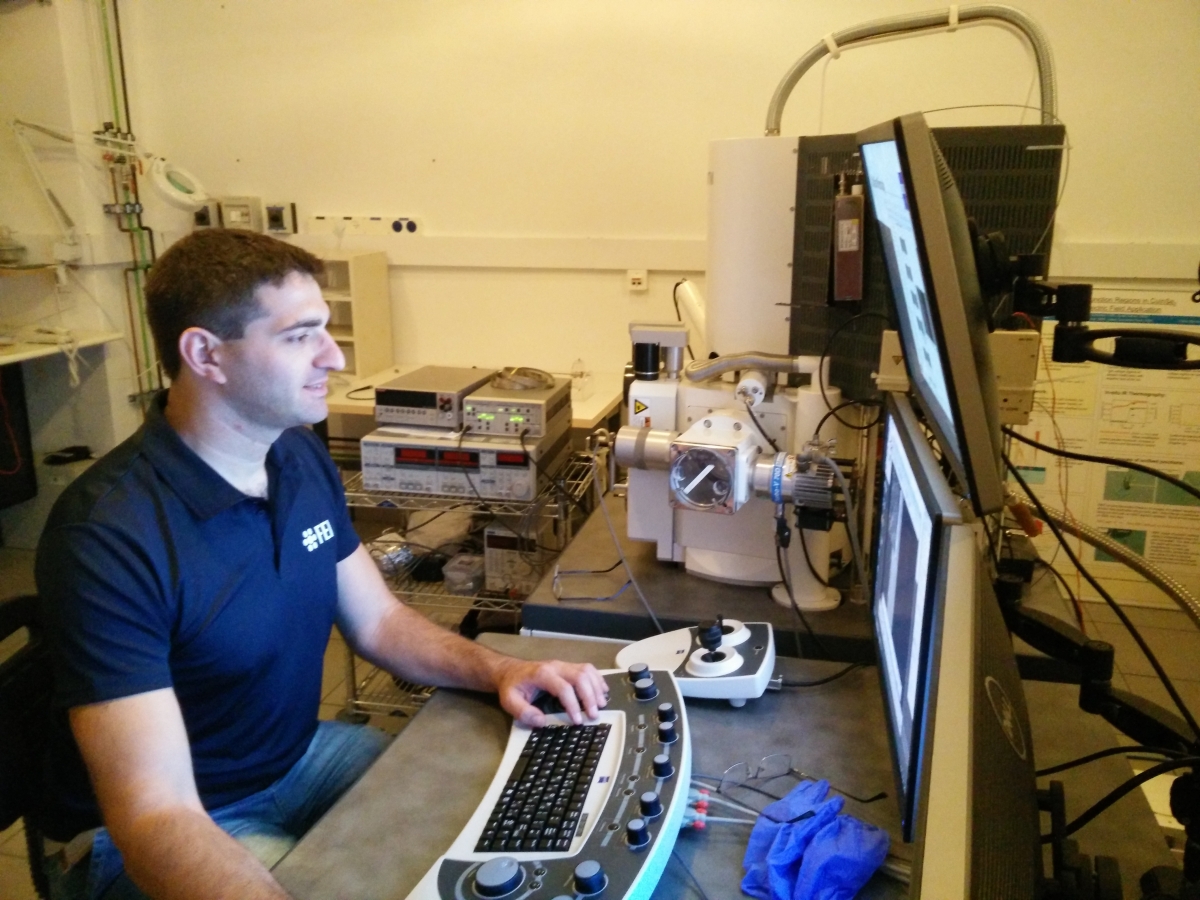
Electron Beam Induced Current (EBIC)
EBIC is a scanning electron microscope-based method used to give an excited-carrier collection efficiency contrast image. As the beam is focused to a nano-probe and the interaction volume with the materials can be as low as a few tens of nanometers, a high resolution image can be produced. The (relatively) highly energetic beam is used to excite electron-hole pairs in semiconductors, which can then be collected at selective electrodes. Collection of the carriers is translated into current at an external circuit, measured, and correlated to the (known) position of the beam on the sample at that time. As the e-beam scans the sample pixel by pixel, high current indicates high collection efficiency and low current suggest poor or no collection.Much information can be gained by mapping the collection efficiency and fitting gradients found in line profiles at the image. First, areas in which highly efficient collection occur, such built in fields (e.g. p-n junction) exists, would be highlighted. Second, an exponential decay rate of the signal is commonly correlated with minority carrier diffusion/drift length. Third, in-situ biasing of the sample and the resulting change in built in fields (space charge region width) can be used to estimate the doping level as well as tracking collection efficiency in a biased device (e.g. at max power point vs. JSC).

Scanning Electron Microscopy (SEM) - imaging and e-beam writing


