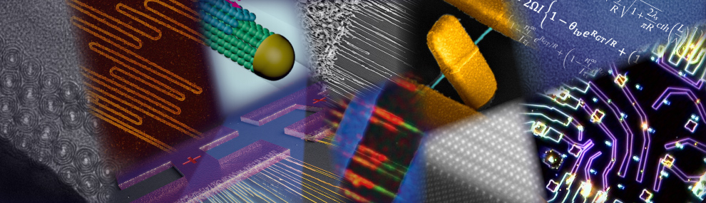
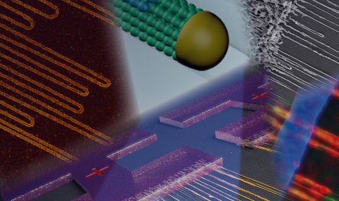
As mentioned at the end of the Overview, besides the self-organization of ordered nanostructures, our second emphasis is on investigating the coupling between different properties, which also enables new functionalities at the nanoscale. For instance, how does an external signal like light or a mechanical deformation affect the electrical conductance of a nanotube or a nanowire? These and other inter-property couplings can be the basis for different miniature devices ("functional nanosystems"), like optoelectronic devices (e.g. photodetectors, solar cells) or nanoelectromechanical systems (NEMS) that could be used as motion sensors (e.g. accelerometers, gyroscopes). Conversely, a device can often allow us to characterize basic properties of nanomaterials. For instance, a field-effect transistor allows us to determine the charge carrier mobility, concentration and sign. A NEMS allows us to study the mechanical properties of nanostructures, including internal details, such as how the coupling between the walls of a nanotube is affected by their chiralities.
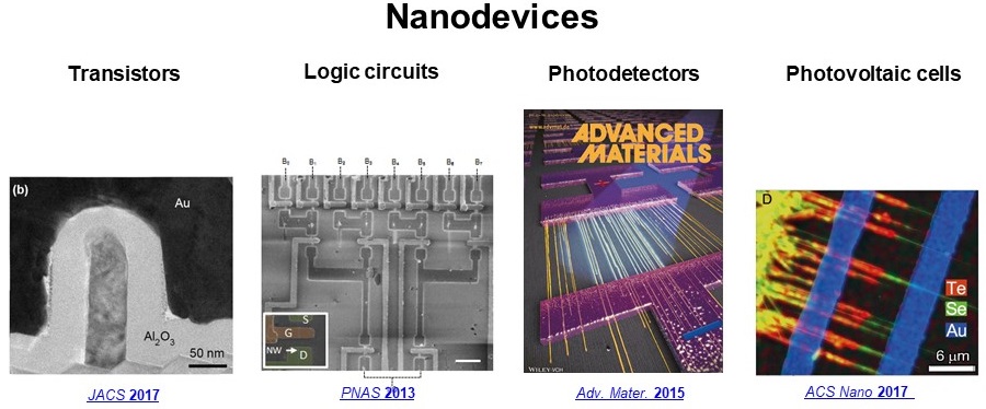
Below are a few examples of functional nanosystems created and investigated in our lab, including electronic, optoelectronic, electromechanical and electromagnetic devices. Current efforts are also aimed at more sophisticated devices for neuromorphic computing (e.g. memristors) and quantum computing (qubits). The fabrication of these devices was made combining nanostructures grown in our lab or other places with micro- and nanofabrication in our clean rooms.

Practical devices
Although our research in primarily fundamental, we also pursue the invention of potentially useful nanosystems for practical applications. These are developed to the proof-of-concept level (TRL 2-3) in our lab. Patents are then filed to protect the inventions, and commercialization efforts or start-up initiatives are pursued for further development together with the Weizmann Institute's IP and R&D branches Yeda, BINA and WIN.