Topological superconductivity realized in hybrid van der Waals heterostructures
Topological superconductivity is a unique quantum phase of matter, not just characterized by the ability to conduct electrical current with zero resistance, but also involving the presence of special boundary states that behave similar to Majorana fermions, particles that are their own antiparticles. These states are called Majorana Zero Modes and their presence in a topological superconductor is tied to the material's unique electronic structure and the interaction between superconductivity and spin-orbit coupling (SOC). This results in protected states that are robust against external perturbations, making them potentially useful for quantum information storage and manipulation. One way to achieve these properties simultaneously is to assemble together a heterostructure of corresponding atomic layers.
To create such a heterostructure one should manipulate different kinds of van der Waals materials, every layer of which is a single-molecular sheet. Thus one may stack together a structure, where one layer is superconducting and another is semiconducting with strong SOC. The materials with required properties can be found among transition metal dichalcogenides (TMDs), a class of compounds, showing various types of behavior from insulators to superconductors.
We study various platforms, utilizing vdW superconductor NbSe2, where it is shaped and stacked together with graphene and other vdW materials. Because of its nature NbSe2 is a perfect material to create highly transparent superconducting contacts, and robustness of its properties allows to use it in high magnetic fields. The spoon of tar here is high sensitivity of NbSe2 to presence of oxygen or water, leading to its destruction. That is why manipulating NbSe2 and creating devices based on it are required to be conducted inside the glovebox with inert argon atmosphere, with both oxygen and water vapors concentration to be kept below 0.1 ppm. Though not being simple to handle this superconductor provides a way to create structures for observation of fascinating phenomena.
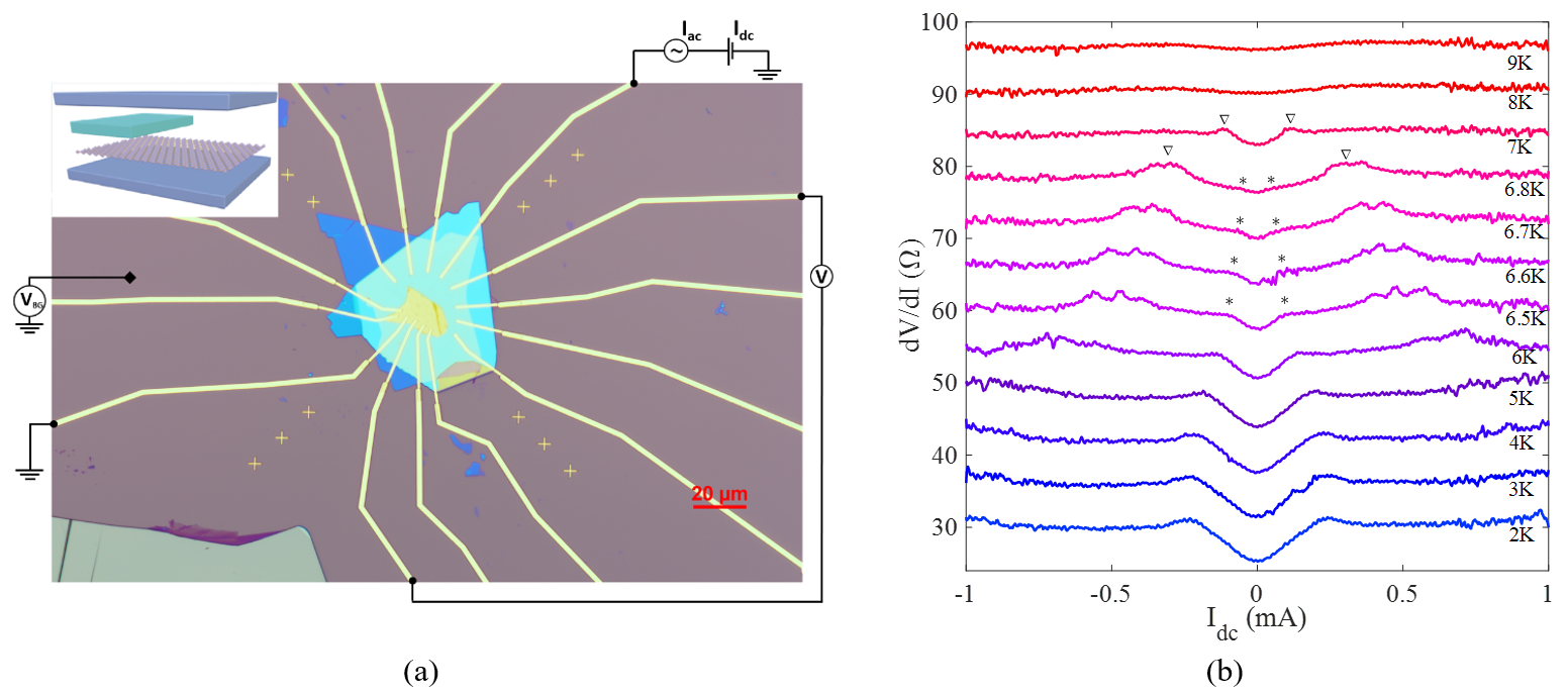
Figure 1. (a) The microphotograph of the encapsulated NbSe2/graphene S-N junction with the measurement configuration; the insert schematically depicts inner structure of the sample. (b) dV/dI (Idc) dependences at different temperatures measured for the sample at Vbg = 60 V, the curves are offset for clarity. The results of the measurements show clearly the proximity-induced superconductivity in graphene.